|
|
NEW PHASE SPLITTER
Phase
Splitters
are essential
in
push-pull
audio amplifiers.
By them
depends largely
the overall
performance
obtainable by an
hifi
audio amplifier. For a long time I thought of a new solution on this issue but clearly the good idea did not come immediately, and several attempts was failed, but after many years, finally I get the good idea, so I started to work on the optimization of the circuits. They come out in different versions so that we can speak about a new entire class of phase inverters, the most significant are included in the document for the patent application. They operate in truly symmetrical and balanced mode, even more than a transformer, (not having its bandwidth limitations also). It's born the phase splitter of the 21st Century !!!! titled "Fully Differential Phase Inverter"
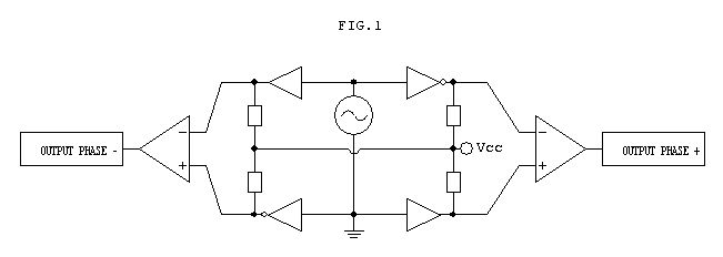
FIG.1 shows the common basic architecture from which were inspired all circuits here presented: an input signal is wired with two inverting amplifiers and also with two non inverting amplifiers. Their relative network is made to form also twin simmetric differential amplifiers with a cross-connection of their inputs at the same time. Then their four outputs drive other 2 differential amps to obtain a convergent syntesis in two output reflecting signals.
Here the simpler versions
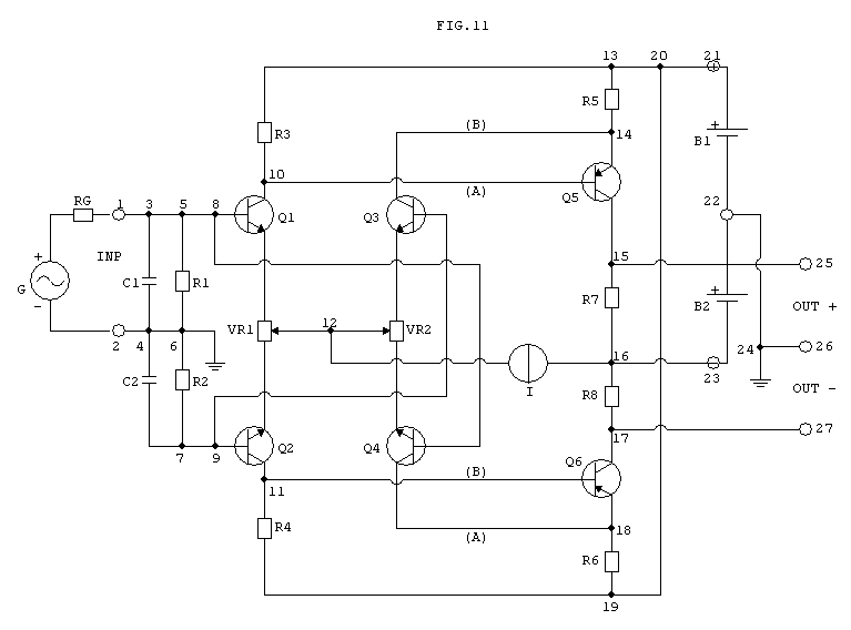
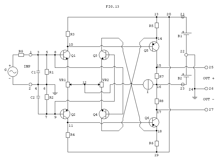
FIG.11 shows the simplified version of those type of circuits that, also maintaining the same FIG.1 principle's structure, have a minimal number of components. This simplified version of the circuit object of application, present dual power supply batteries (B1, B2) or equivalent, six active devices of amplification (Q1, Q2, Q3, Q4, Q5, Q6) including bipolar transistors (BJT) or unipolar transistors (JFET, VFET, MOSFET, SIT and the like), one constant current source (I), two trimmers (VR1, VR2) two input resistors (R1, R2), two capacitors (C1, C2), six load resistors (R3,R4,R5,R6,R7,R8), two signal input terminals (1-2), three output terminals (25-26-27), three power supply terminals (21-22-23). A signal generator (G) is applied with the polarity shown between the terminals 1 and 2 while the signal supplied to the utilizer is taken between terminals 25-26 for the positive phase and 26-27 for the negative phase, being 26 the common ground terminal. For FIG.11, ( and following FIG.12 and FIG.13), we define these features: 1. transistor Q1 = Q2 = Q3 = Q4 ; 2. transistor Q5 = Q6; 3. resistor R3 = R4; 4. resistor R5 = R6; 5. resistor R7 = R8; 6. resistor R2 = R1// RG Referring to FIG.11, it is observed that the bases of Q1 and Q4 are connected, through nodes 8,5,3 and terminal 1, to the positive phase of signal generator G, while the bases of Q2 and Q3, through nodes 9, 7, resistor R2 and node 6, to the ground signal. At the same ground, through terminal 2 and nodes 4 and 6, is connected the other end of the signal generator G (the negative phase). Consequently, we can observe that the network in which are inserted the aforesaid transistors Q1, Q2, Q3,Q4 form a multiple differential amplifier. In particular we can see two vertical differential amps of which the first formed by the pair Q1,Q2 and the second formed by the pair Q3,Q4. At the same time with the same network and the same four devices we can see also two horizontal differential amplifiers, of which the upper formed by Q1,Q3 and the bottom formed by the pair Q2,Q4. In addition, for the created network, there are two further simple differential amplifiers the first of which formats by transistor Q5 (for the upper branch) and the other by Q6 (for the lower branch); Q1 collector through node 10 is connected to base of Q5, Q3 collector to emitter of Q5 through node 14, and, on the lower branch, collector of Q2 through node 11 is connected to base of Q6, while collector of Q4 is connected to emitter of Q6 through node 18; finally, collector of Q5 through node 15 is wired to output terminal 25 and collector of Q6 via node 17 is connected to output terminal 27; terminal 26 connected to ground through node 24 is also the reference for the output signals present on terminals 25 and 27. Applying a signal between input terminals 1, 2, with the polarities as indicated we obtain two signals equally amplified in voltage on collectors of transistors Q1 and Q4 (nodes 10, 18), with negative phase, which we will call signal (A), while on both collectors of transistors Q2 and Q3 we get two equal signals also amplified in voltage (generally a bit different from the first), with positive phase, which we will call signal (B) (nodes 11, 14). It follows that base of Q5 receives a signal (A) identical to that received from emitter of Q6, while emitter of Q5 receive a signal (B) identical to that received from base of Q6. Forming each of said transistors Q5 and Q6 a differential circuits where the amplification coefficient is proportional to the sum of the signals (A) and (B) present on the respective bases and emitters, it follows that the signals on the collectors of transistors Q5 and Q6 (and then on the outputs 25 and 27) will be amplified at the same level of amplitude but with opposite phases. It is also noted, as a result of the circuit’s symmetry, that the frequency response, the output impedance and any other parameter of the two signals provided are very coincident. For the same reason, this proposed circuit can also boast of a good external noise rejection and a good behavior against power supply noise, as well as a low intrinsic distortion. A further advantage, compared to existing phase-inverters, is the not negligible property of being able to be free of DC voltage (offset) at its outputs, which obviates use of capacitors between its outputs and user equipments.
You think that, although more accurate, this phase splitter is more complicated than others? No, it is not entirely true and I will prove that in the following application of this one in a high power circlotron amplifier. It must be recognized that this circuit replaces the work as many as 3 stages used in more conventional design. In fact it performs and replaces:
At the end this schematic is rather simple. Let me know any more simple for 300 W !!!
Now we continue with other versions.
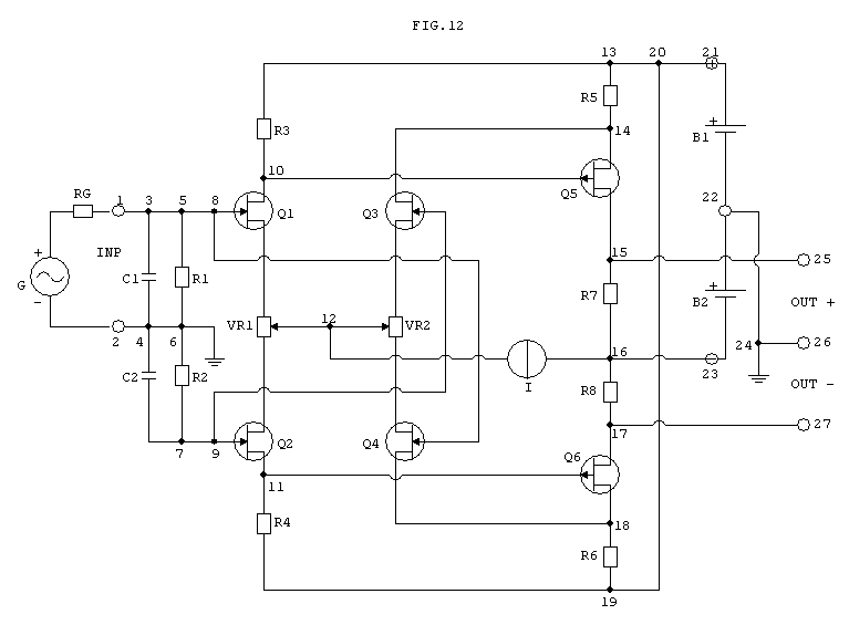
In FIG.12 is presented a version circuit derives from that in FIG.11 utilizing unipolar JFET devices, instead of transistors, as example
FIG.13 is instead a variant of FIG.11, in which they were exchanged collector’s connections between transistors Q3,Q4 to transistors Q5,Q6 in order to decrease the value of the total amplification rate. In fact it not should forgotten that the circuit of FIG.11 has a high coefficient of amplification in that the pair Q1,Q3 connected to Q5, and Q2,Q4 connected to Q6, on the lower branch, form two identical push-pull folded cascode circuits.
In the following the more accurate balanced version
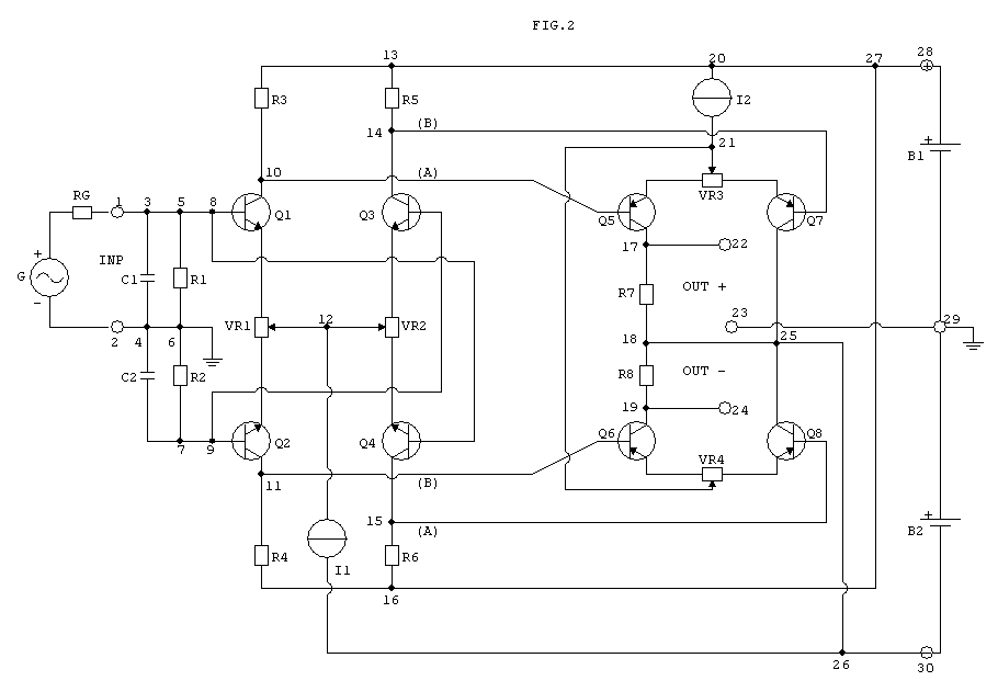
FIG.2 illustrates the complete application circuit in which are transferred in a practical way the ideas expressed in the principle’s schematic of which in FIG.1. For circuits of FIG.2,(and the following FIG.3/4/5/6/7/8/9/10) are valid the below relations (if any): · Q1 = Q2 = Q3 = Q4; · Q5 = Q6 = Q7 = Q8; · R3 = R4 = R5 = R6; · R7 = R8 = R9 = R10; · VR1 = VR2; · VR3= VR4; · R2=R1//RG Referring to FIG.2 and, for the above statement, it is noted that the input circuit is formed by two symmetrical differential amplifiers either coupled by emitters (first bridge circuit). It is noted first that it is equivalent to describe the two differentials as formed by the pairs of transistors Q1,Q3 (high) for the first differential and Q2,Q4 for the second (bottom), rather than formed by pairs Q1,Q2 (left) for the first differential and Q3,Q4 (right) for the second differential. In conclusion the circuit in question can be equivalently decomposed into two differential circuits in vertical, horizontal or cross-connected mode. The important point to note is that, we could breaks down the circuit, still having input of said first differential connected to the hot pole of the signal generator G and the other input of the same differential amp connected to ground (cold), while the second differential amp will always have one input connected to the hot pole of the generator G and the other to ground but in reversed order compared to the first differential, so that the two differential amps have their input cross-connected. The second stage is also formed by twin emitter coupling differential amps (second bridge), thus the output impedances seen by the four transistors Q1, Q2, Q3, Q4 are identical. Referring to FIG.2, the base of Q1 is connected to the G hot pole (1), through the nodes 8,5,3, while the base of Q3 is connected to the cold pole (2) of the same generator G through nodes 9,7, the resistor R2, then nodes 6,4 and therefore connected to ground; vice versa, the base of Q2 is connected to the cold pole (2) through said nodes 9,7, the resistor R2 and the remaining nodes 6,4, while the base of Q4 is otherwise connected to the hot pole (1) of signal generator G through the aforesaid nodes 8,5,3; then the collector of Q1 through node 10 is connected to R3 which then through nodes 13,20,27, and terminal 28 reach the positive pole of battery B1; the collector of Q3, arrives via node 14 to the resistor R5 whose other end is connected to the node 13 and from this through the cited nodes 20,27 and terminal 28 reaches the positive of B1 battery; the Q2’s collector through the node 11 is coupled to resistor R4 whose other end arrives, through nodes 16,27, and the predicted terminal 28, to the positive battery B1; the collector of Q4 via the node 15 is connected to R6 which in turn is connected to the nodes 16 and then 27 and from this to terminal 28, where it is connected to the positive pole of B1 battery; the emitter of Q1 through VR1 is connected to node 12; the emitter of Q3 through VR2 is also connected to node 12; the emitter of Q2 through VR1 is also joined to node 12; the emitter of Q4 through VR2 is connected to the predicted node 12 which is connected to one end of the constant current source I1, the other head of I1 through the node 26 is connected to terminal 30, that is the negative pole of the B2 battery, the node 10 wired to base of Q5, the node 14 to base of Q7, the node 11 to base of Q6, the node 15 to base of Q8; node 20, carries the positive voltage to one end of the constant current source I2 whose other end is connected to the central contacts of VR3 and VR4 whose external contacts of the two trimmers are connected to the emitters, respectively, of Q5, Q7 and Q6, Q8; collector of Q5, via node 17 reaches, by one side the output terminal 22 (phase +) and, from the other side, the load resistor R7, which is then connected to the node 18, then it is is connected the other load resistor R8 and by this to the node 19, where there is a first connection to the output terminal 24 (phase -) and a second to the collector of Q6; the collector of Q7 is connected directly to node 25 and then to the collector of Q8; node 18 is connected to node 25, then to 26, and finally to terminal 30 that’s the negative B2 battery pole; the remaining output terminal 23 is connected to terminal 29, the central connection among the two batteries B1 and B2 and from this, connected to the ground system. For a common understanding, we suppose in the following to refer as differential amplifiers formed by horizontal pairs. By applying an input signal with the polarity indicated, on the collectors of transistors Q1 and Q4 (10,15 knots), working these BJT as common emitter amps, we get two identical signals both shifted by 180° with respect to the reference of G, which we call signal (A) ; simultaneously on the collectors of Q2 and Q3 (11,14 knots), operating these devices as common base amplifiers, we obtain two equal signals between them and in phase with the reference input signal of G, which we denote as signal (B). The upper node 10 is connected to base of Q5, the node 14 to base of Q7, while on the lower branch, the node 11 is connected to base of Q6 and the node 15 to base of Q8, therefore it is apparent that the pair Q5,Q7 receive a pair of signals (A) + (B), while the pair Q6,Q8 receive a pair of signals identical to the first but in reverse order, hence (B) + (A). In fact, the transistor Q5 receives directly on its base the signal (A) and on emitter, through Q7, the signal (B), while the transistor Q6 receives directly on its base the signal (B) and on emitter through Q8 it receives the signal (A), instead. Forming both pairs Q5,Q7 and Q6,Q8 two differential amplifiers, (whose outputs are function of these two input signals (A) and (B), on the collectors of Q5 (nodo17) and Q6 (nodo19) we obtain two signals, which, although identical in every other electrical parameter, are however in phase opposition by 180°, which it is the result sought. These signals are withdrawable on terminal 22 (phase +) and 24 (phase-) with terminal 23 bonded to ground act as common reference for both. The outputs are also reported to zero DC voltage and this allows a direct coupling of the invention to the user circuit. It is also noted that, as a result of the symmetry of circuit, the frequency response, the output impedance and any other parameter of the out signals are perfectly coincident. For merit of this, the proposed circuit can also boast of a good external noise rejection and a good behavior against power supply noise, as well as a low intrinsic distortion. Excluding the sign, the mutual phase delay and the time slider between the two supplied signals is zero, ie, they are perfectly synchronous.
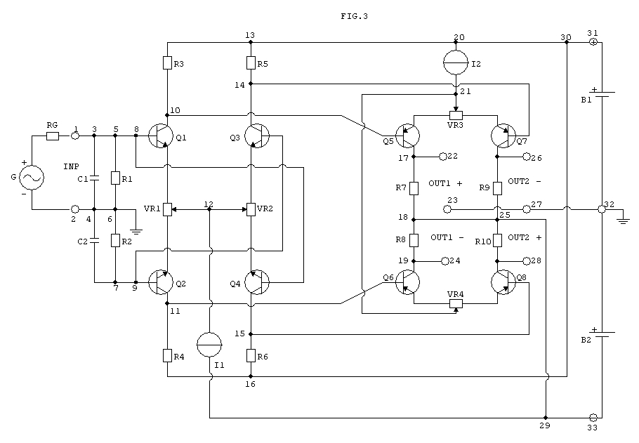
The circuit depicted in FIG.3 derives directly from that of FIG.2 where the second stage is also formed by two pairs of symmetric differential amplifiers, rather than asymmetric, as in the previous case (it have been added the resistors R9 and R10), and this allows, for the first time in this kind of circuits, the possibility to quadruple the number of output signals (four signals in pairs with the same phase). As in the previous case, these four signals, apart from the sign, are all synchronous.
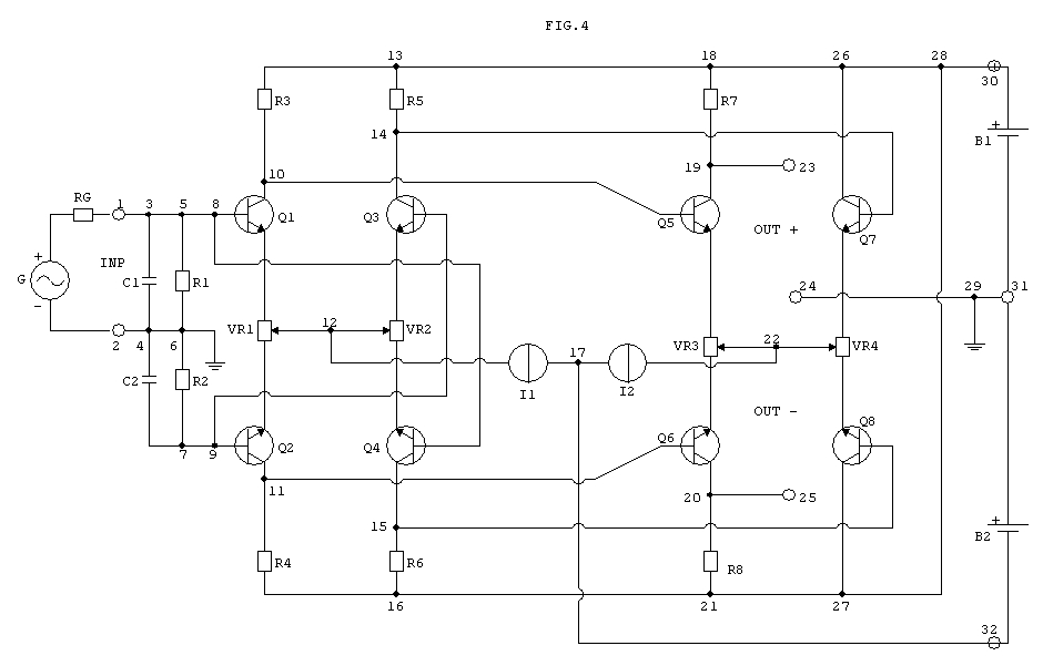
The circuit of FIG.4 is derived from that of FIG.2, when we must use only devices of the same polarity. (NPN or PNP, in this figure all N-channel). It represents a solution when you want to achieve this phase shifter with all vacuum tube devices (triodes, pentodes) or with other devices of which there is no complementary counterpart.
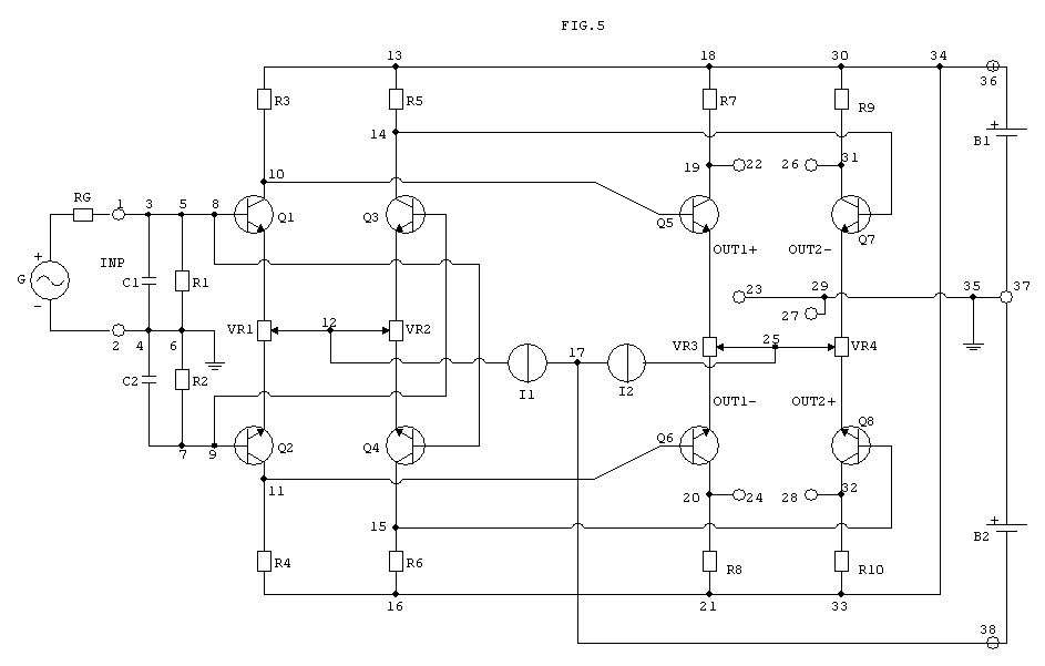
The circuit of FIG.5 is a direct descendants of FIG.4 that provides up to four outputs with the output phases as shown.
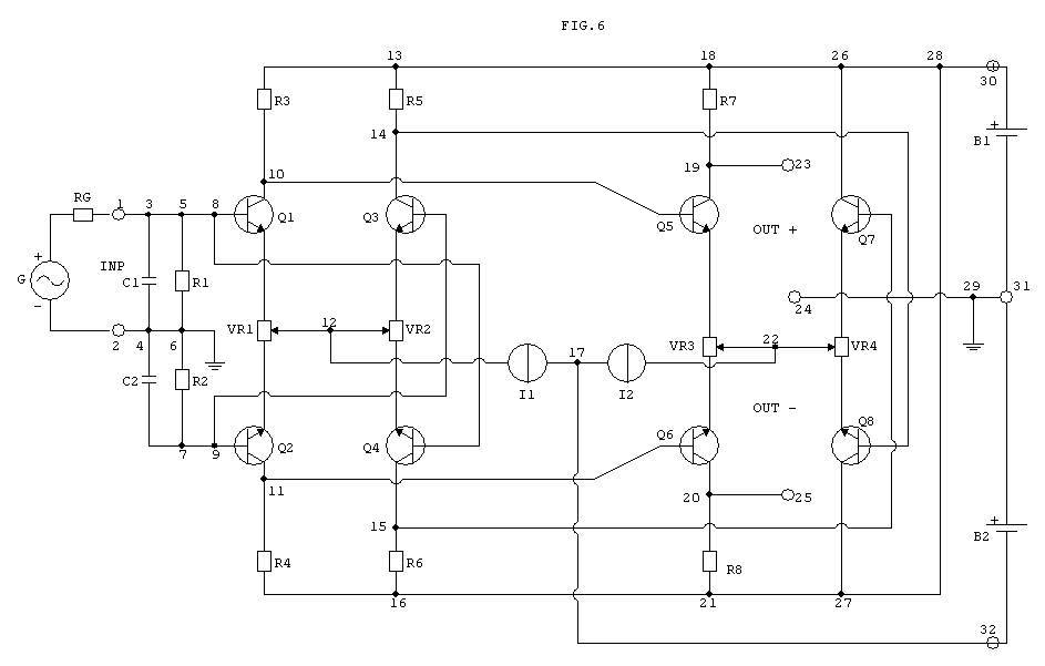
In the circuit of FIG.6 it have been exchanged some connections compared to those of FIG.4, whose phases output, as shown, reveal that it is perfectly equivalent to this latter.
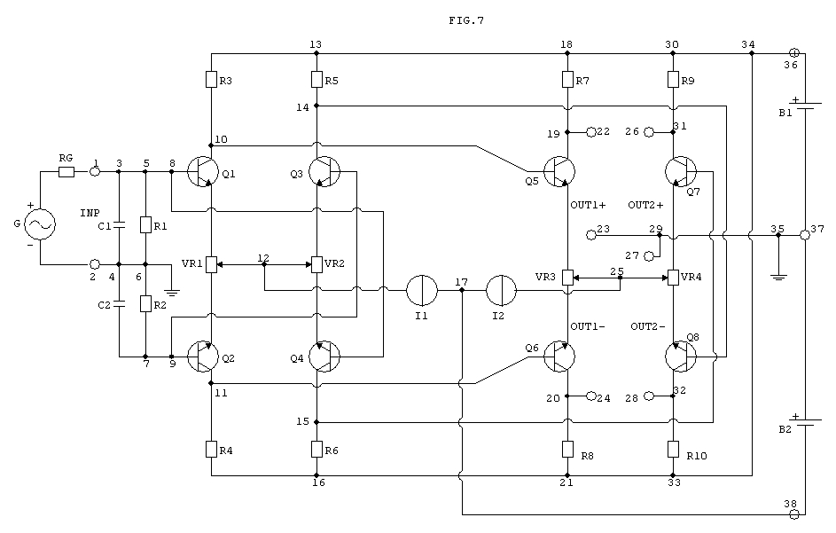
The circuit of FIG.7 follows directly from that of FIG.5, where, with respect to this, it have been exchanged two of the four wires which carry the signal from the first group of differentials (first stage) to the second group (second stage). This operation just swap the order of the output phases but everything else is perfectly equivalent to the former in FIG.6 It is shown by way of example.
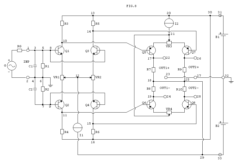
Circuit of FIG.8 derives from that of FIG.3 having different input connections of the first stage: At first sight it not seems to found differential amps, indeed we can view several vertical diff. amps: Q1 with Q2, Q3 with Q4, Q5 with Q6, Q7 with Q8.
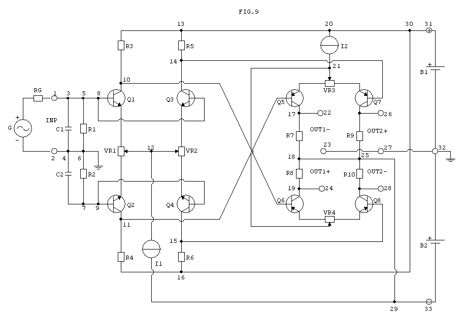
Circuit of FIG.9 descends directly from that of FIG.8 in respect of having cross-connections from first to second stage.
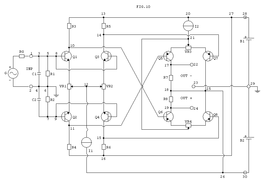
Circuit of FIG.10 is a two output version of that in FIG.9
In the following some main features:
its outputs;
If you or your company have interest in this last
application, please contact me:
E-mail: info@amplimos.it
These circuits are know overall in audio application (preamplifier and push pull amplifiers, unbalanced to balanced signals in professional audio gear),but also in Switched Mode Power Supply, in instrumentation and other fields of science and physics. |