|
|
|
V-FET and SIT
The static induction transistor (SIT) is a three-terminal semiconductor device. Similarly to other active devices (like the bipolar-junction transistor (BJT) or the junction field-effect transistor (JFET), in a SIT the current flow between two terminals (the source and the drain) can be controlled through the third terminal (the gate). Static induction transistor (SIT) was invented by Y. Watanabe and Professor Junichi Nishizawa of Tohoku University in 1950 with a multichannel structure; it controlled current flow by means of the static induction or electrostatic field surrounding two opposed gates. Many years passed before transistor fabrication technology was sufficiently developed to take advantage of this concept. In 1975, however, experimental SITs were fabricated and the source-drain current of this device was shown to follow the predicted space-charge injection model. Static induction transistor (SIT) shows non-saturating I-V character and high-frequency and high-efficiency characteristics as the result of the reduction of the series channel resistance. SIT has a caged type gate electrode similar to the grid in vacuum tube triode and the electro-static potential around the gate electrode control the flow of majority carriers).
The idea was so innovative that the current establishment in the solid state
electronics community had difficulty understanding and accepting this discovery. As said the SIT has been originally conceived as a solid-state analog of the vacuum-tube triode. The device is normally on, and a reverse bias applied to the gate is used to modulate the drain-source current. In this mode of operation the steadystate current drawn from the gate is negligible, and the SIT can be considered as a voltage-controlled device, like the JFET.
A SIT, however, can also be designed to operate with a forward bias applied to the gate terminal (in this case, the device is called bipolar-mode SIT or BSIT). In this mode of operation a significant current flows through the gate of the SIT and the device becomes current-controlled, similar to a BJT. The BSIT is generally designed as a normally off device and is characterized by a much larger current-handling capability with respect to SIT. SITs are a class of transistors with a short-channel FET structure in which a current flowing vertically between source and drain is controlled by the height of an electrostatically induced potential energy barrier under the source. This electrostatic barrier develops at pinch-off when negatively charged opposing gate depletion layers coalesce to completely deplete the source-drain channel of mobile charge carriers. Analogous to the vacuum triode, both the gate (grid) voltage and the drain (anode) voltage affect the drain (anode) current because, in the SIT, the height of the induced electrostatic barrier is influenced by both these potentials. By 1969, it became a complete device having non-saturating type voltage/current characteristics. One of the main advantages of the SIT device is its high speed switching characteristics. Since no carriers are injected from the gate, switching can be performed at an extremely high speed (without storage effects) and a small gate resistance (rg) is used for minimum high frequency signal loss. SIT have high input impedance and is a voltage controlled device and therefore low drive power is required at the gate. The absence of electric current concentrations for very high breakdown voltage resistance can be explained by the negative temperature coefficient of the drain current, due to some residual channel resistance, which makes it difficult for thermal runaway to occur. Thus SITs are highly suited for high power applications. The non-saturating current/voltage characteristic is based on the SIT exponential function characteristics due to their reduced negative feedback capacitance. SITs can be defined as a type of V-channel field effect transistor (FET) in which the distance between the source and depletion layer of the drain is so reduced that the negative feedback of the channel resistance will not affect the direct current characteristics. SITs require a negative voltage signal in order to turn off as they are normally-on devices. They can operate as a unipolar or bipolar device (BSIT). Generally, the unipolar mode is used for high frequency applications whereas the bipolar mode is utilized for circuits handling high power. Reason being, the bipolar mode requires the removal of minority carriers from the bulk substrate, which takes more time, thus maximum frequency is reduced.
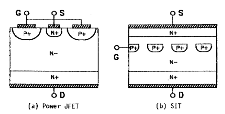
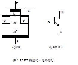
However static induction transistors presented here are normally-ON devices, meaning they require the application of a negative gate voltage signal (respect to the positive main voltage Vds) (Vds and Vgs may be opposite) in order to turn the device OFF. In the SIT structure, the gate voltage controls the current flow through the means of depletion regions that extend from the gate junctions into the n-type channel, extending deeper as an increase in the magnitude of the negative gate-to-source voltage. When the device has zero gate voltage or a small negative gate voltage, a small depletion region forms between the p+ / n- interface, and the channel that forms has a width of the distance between the two depletion regions. With a positive drain-source voltage, majority carrier electrons flow from the source to the drain. With large applied voltages and currents, a resistive voltage drop occurs along the length of the channel, causing a distortion in the width of the depletion layers. If the pinch-off voltage Vp is applied to the gate and a large drain to source voltage is applied to the device, full pinch-off does not occur, and current will continue to flow. In order to guarantee full pinch-off under high Vds operation, a voltage must be applied to the gate that is more negative than the rated pinch-off voltage of the device. The requirement of a negative gate voltage is essential to proper device operation. This latter characteristic is usefully exploited in the production of audio amplifiers in class B or AB because unlike other devices it virtually never turned off completely and therefore also in this mode of operation does not pass completely by the on-state to the off one with all benefits on the sound for the failure to produce artifacts due to oscillations that otherwise would be generated by switching between the aforementioned states. So a Static Induction Transistor (SIT) is basically a power JFET with a buried gate, as shown in Figure b. Construction as well as operation is reminiscent of a vacuum tube. V-FET is a V-groove JFET. SIT has an embedded meshlike grid
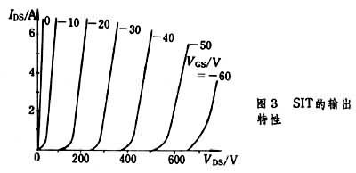
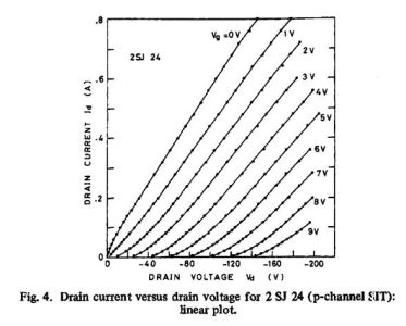
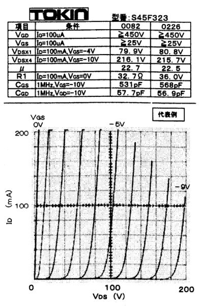
Other SIT construction and electrical symbol. Typical output characteristics of SIT (n channel) Output characteristics of Yamaha 2SJ24 (p channel)
I became interested in SIT (Static Induction Transistor) since 1985, when an Italian magazine (ELETTRONICA OGGI) did an interesting article about these new devices and their excellent characteristics that promised incredible performance in the field of industrial electronics, telecommunications to very high frequency and in the field of the electronics of low-frequency (audio-frequency amplifiers). In particular for the latter use was captured by the dream of one day come into possession and build around the magnificent power amplifiers for use Hi-Fi. Advantages of using audio could be seen for three main characteristics:
I could list other prerogatives, as the increased stability of
operation when the temperature varies or the low output impedance, but from the point of view of audio,
these three points described above are fundamental, all the rest is a more. And Internet? At that era Internet do not existed or were very little information around. For a while the mystery behind the VFET was obscured by lack of data and curves. However since then I have done continuous researches without find anything about. After several years of unsuccessful attempts, finally begins to find some news about it. People began to realize that SIT and V-FET had a lot in common. Indeed they could be considered synonyms as they had the same operating principle and the same type of curves (triode like), as well as the same inventor.
In the audio field such devices were known as V-FET (mainly by Sony) referring to the construction technology, the "V-shaped vertical channel" (see diagram above), while in industry were known as SIT stands for Static Induction Transistor referring to the physical principle relative to the "ELECTROSTATIC" field which with its "INDUCTION" governs the operation. At the end with the names V-FET, VJFET and SIT we intend the same class of devices. If we thinking about applications for which they are intended, today there may be a subdivision:
With the enlargement of the family, it grew in theory the chances of finding someone around. But the search proved very difficult because even despite the production of " Vfet audio amplifiers" in the '70/80 by Sony, Yamaha, Sansui, Hitachi, Wega, JVC many users complained of not being able to repair their failed equipment due to lack of parts of such special devices. However, with time and stubbornness
I managed to make some spare for my accomplishments, as well as I have given
news in some important forum to allow other fans to get hold of them and make
his own V-FET amplifier.
For other VFet amplifiers made by me you must look in the "DIY SCHEMES" page. However, on this page I want to
submit some V-fet schematics that I have proposed in the past on the
aforementioned forums related to a user's request that required V-FET amp
design not using complementary pairs.
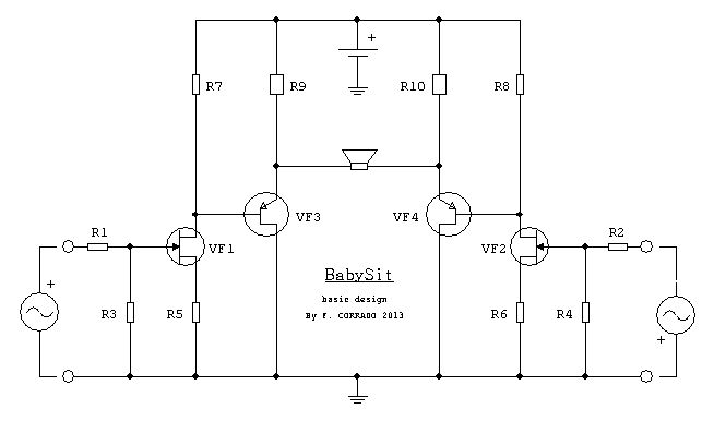
The following circuits are however very interesting and original, as well as very simple to implement, especially because they require a power supply section very simplified compared to other V-FET schematics that require up to 6 or more power supplies because of the different polarity of the Vds with respect to Vgs as mentioned above. In the basic scheme that you see below, circuit needs even only a single power supply. For a push-pull (balanced) V-FET amp I do not think there can be some simpler schematic with fewer components!
Click on the button below to see:
Being uncertain in the parasitic
capacitances of Vfet model used in simulator, all frequency responses have not
been intentionally published, but it is expected to be good if not excellent
within the audio band.
How to test V-FET 1) with multimeter By this first simple mode you can check if it is a genuine V-FET. (example here is for N channel Type (2SKxx). With a multimeter on diode function (for N devices) put positive terminal on gate and negative on the source one time and on the drain last time: everytime you must measure a pn junction (0,4-0,5V). You must measure the 0,4V of pn junction voltage either among gate to source and among gate to drain. Then with a multimeter on resistance function, across Drain to Source you must measure a resistance of about 0,5-1,5 Ohm
That is similarly to measure a signal jfets.
For P channel Type (2SJxx) you must invert the multimeter terminals (negative on gate and positive one time on drain and then on source).
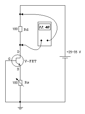
2) in circuit To verify these devices in deep you need a little circuit with: (Example is for N devices)
It is better if you put device on a heatsink
Operations
Generally, the N Vfets are going in on state when the Vgs is lower than -15V but is depend on model and rank (-5V at least)
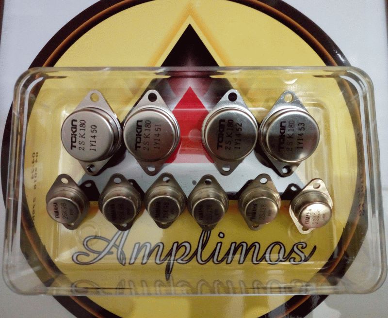
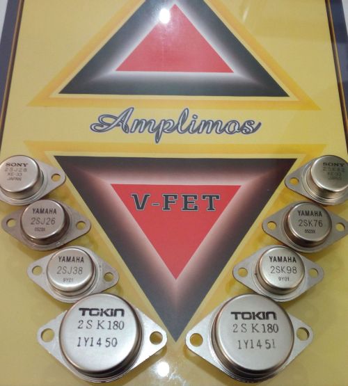
LIST OF V-FET OR SIT TRANSISTORS
4 NEW V-FET SCHEMATICS WITH VERY LOW DISTORTION The diagrams that follow have been developed and simulated in the last year with the intention of realizing amplifiers with the greatest possible linearity (low distortion), to better enhance the use and the role of Vfet in medium power audio applications. Before proceeding with the description of the different circuits it should be noted that at the moment they are only simulated and not realized practically. From this, it follows that the undersigned assumes no responsibility for any malfunctions and negative consequences caused by the realization in their own of such projects (DIY) .
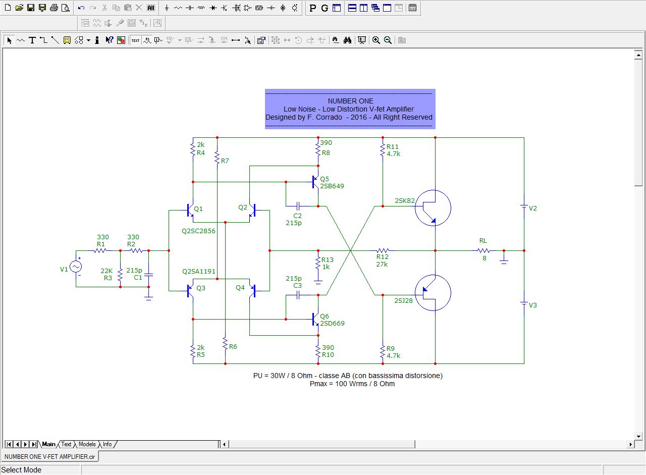
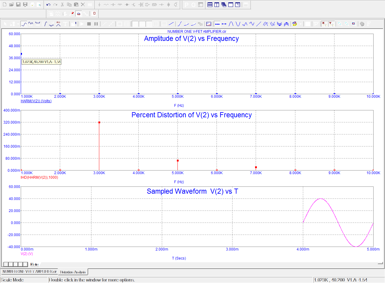
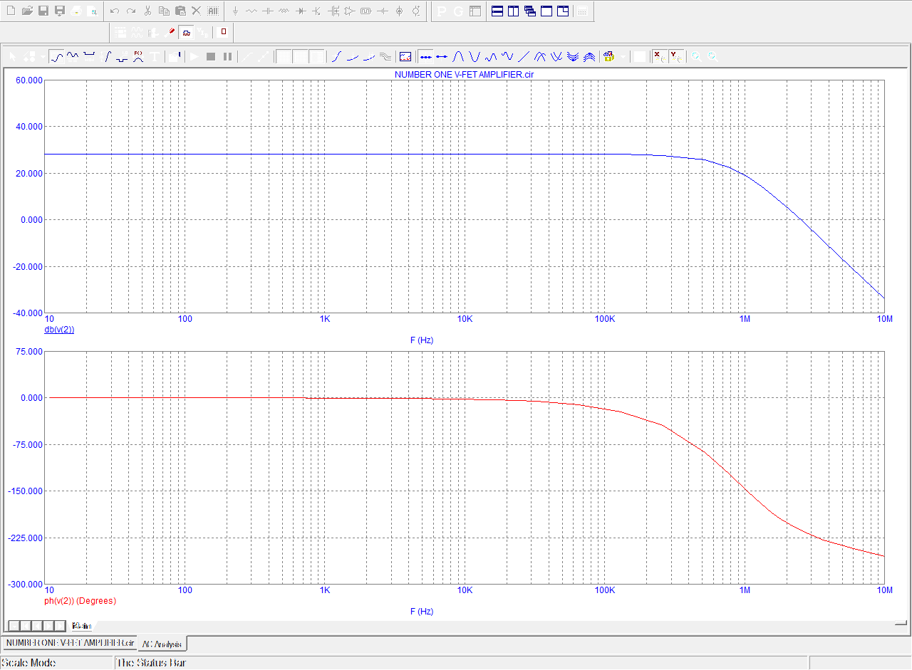
The first scheme I intend to bring to your attention could only be called "NUMBER ONE", the first, in fact. It is a directly coupled complementary symmetry circuit up to 100 watts of rms power into 8 ohms, but more importantly, it has a very low harmonic distortion over all the power and particularly excellent up to 35 watts effective. These values are obtained in spite of the class AB operation and with the use of moderate global feedback . The power supply system is also quite simple and involves the use of a dual power supply. An easy to build amplifier, with good power for domestic use and excellent performance. Notes.: This amplifier is designed for 8-ohm speakers. If you plan to drive loads of 4 ohms it must be added another pair of V-FET. In this case the maximum power could reach 200 Wrms.
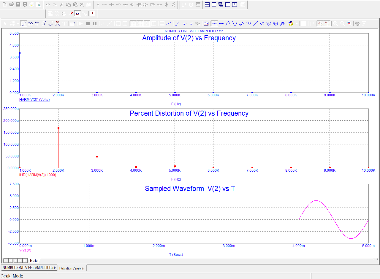
In the above: spectrum of the distortion at 1W
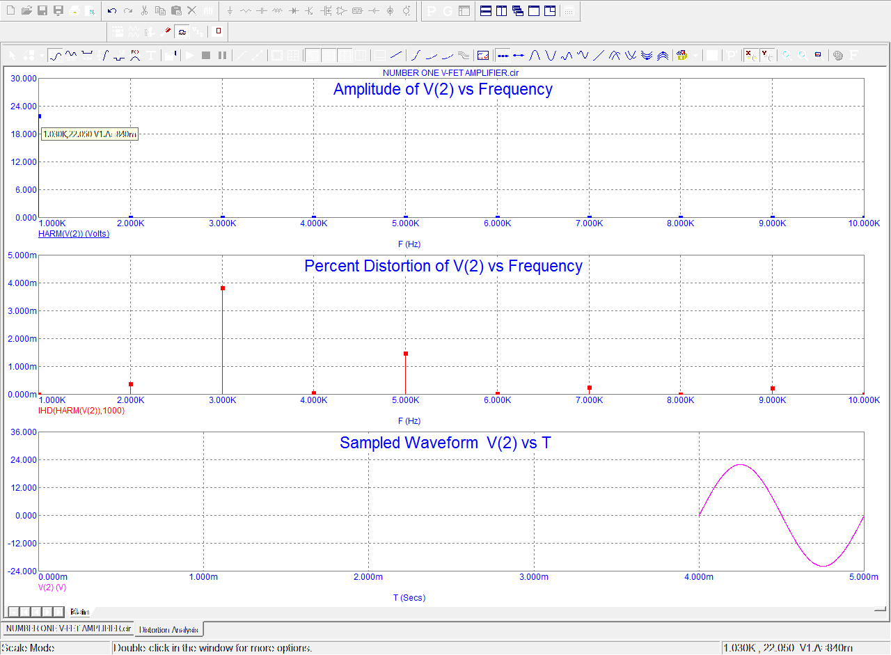
above: distortion spectrum at 30W
above: distortion spectrum at 100W
frequency response and phase response
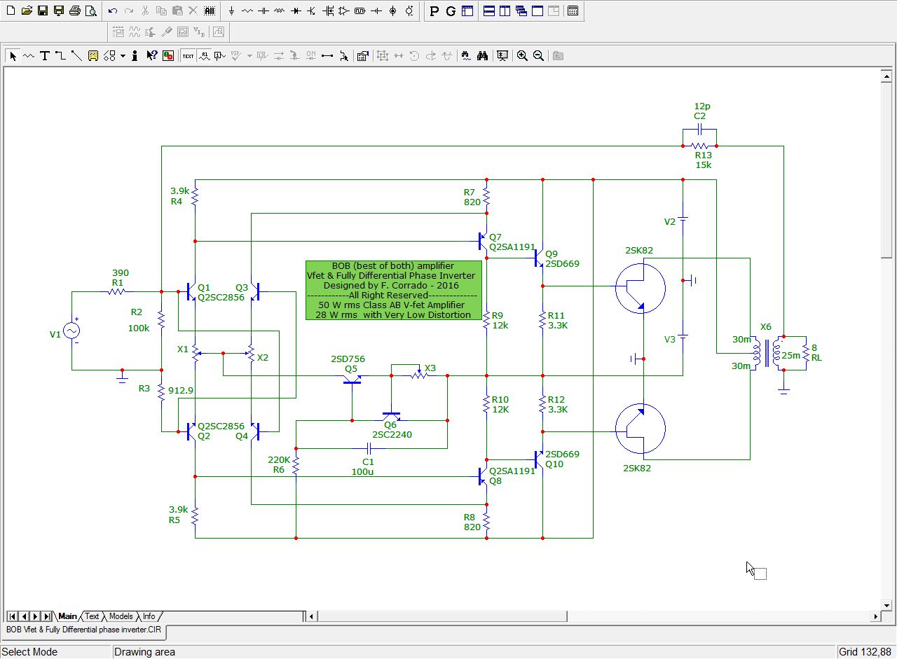
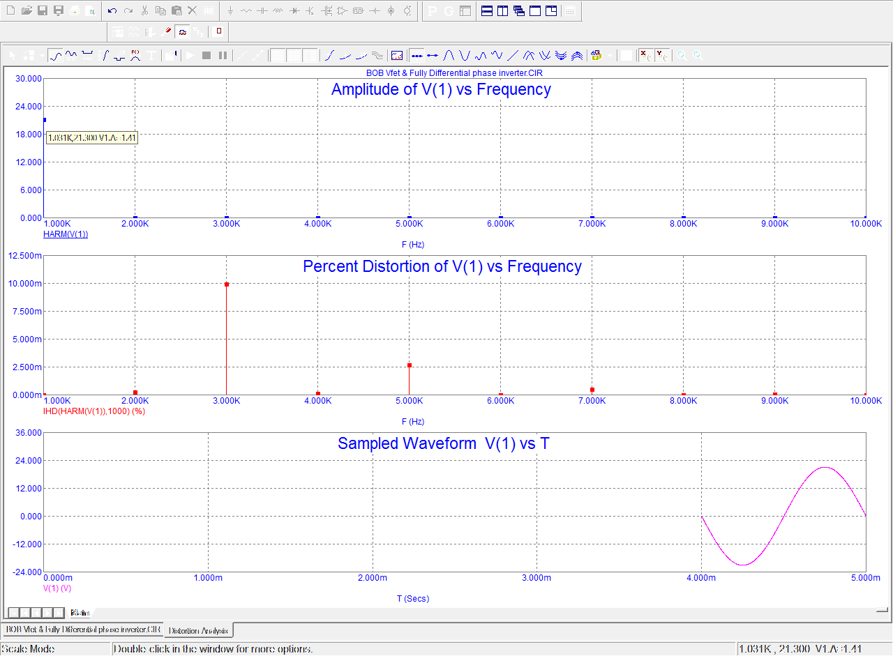
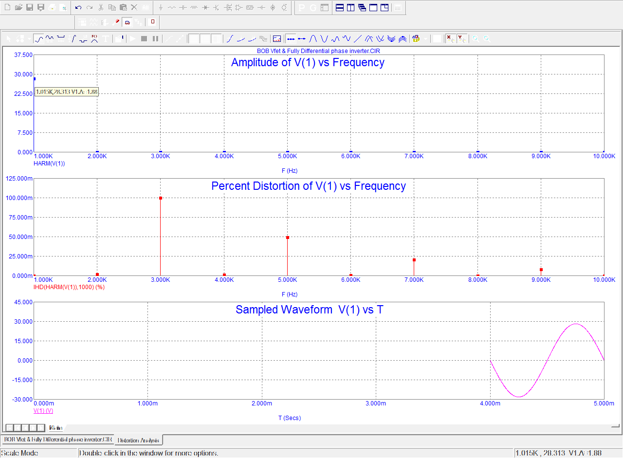
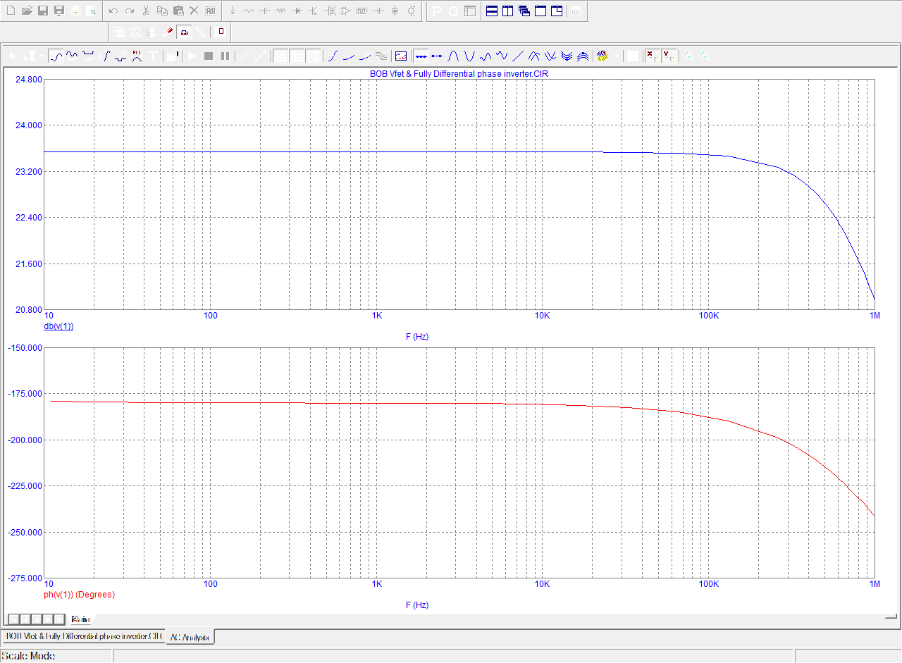
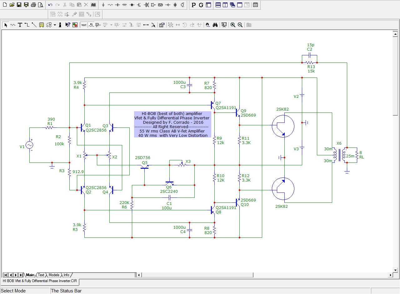
The second circuit that I present is called "BOB" initial of "Best of Both" world, that is best of that tube circuits and semiconductor circuits.
By the first it uses the output transformer and the
use of devices of an identical polarity in the two branches of the push-pull,
giving a better balance of the signal. Everything is driven to the level of further excellence through the use of a special phase splitter (in my opinion): the Fully Differential Phase Inverter. It allows a perfectly balanced driving signal of the power devices with positive effects on the linearity and purity of the output signal.
The power is greater than 50 W rms into 8 Ohms,
with a very low distortion profile, particularly within the first 28Wrms / 8. Notes: This amp is designed for 8-ohm speakers. For loads less than that it is advisable to double output pairs. Consequently the achievable power could increase or doubling
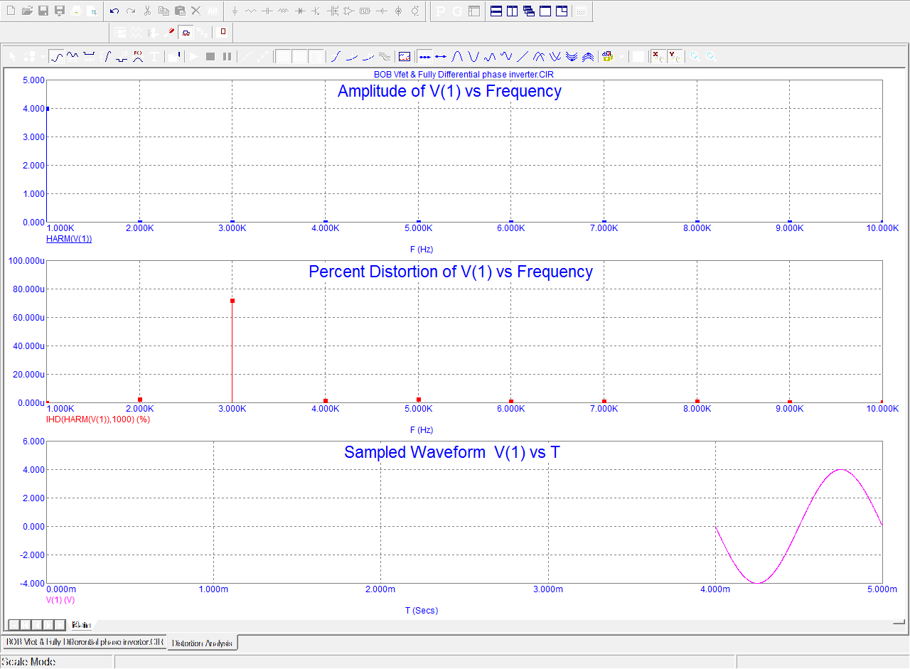
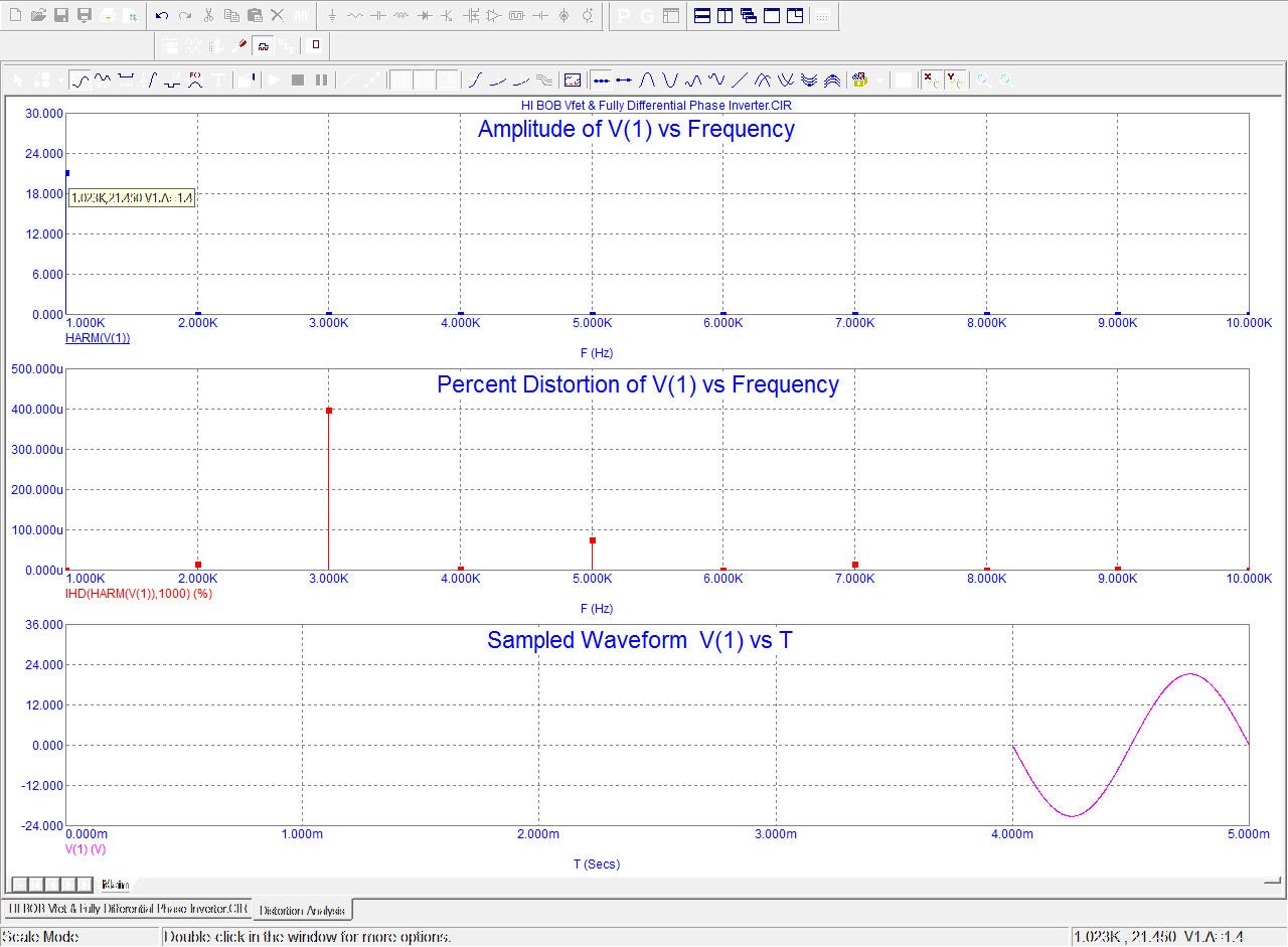
above: harmonic distortion at 1W
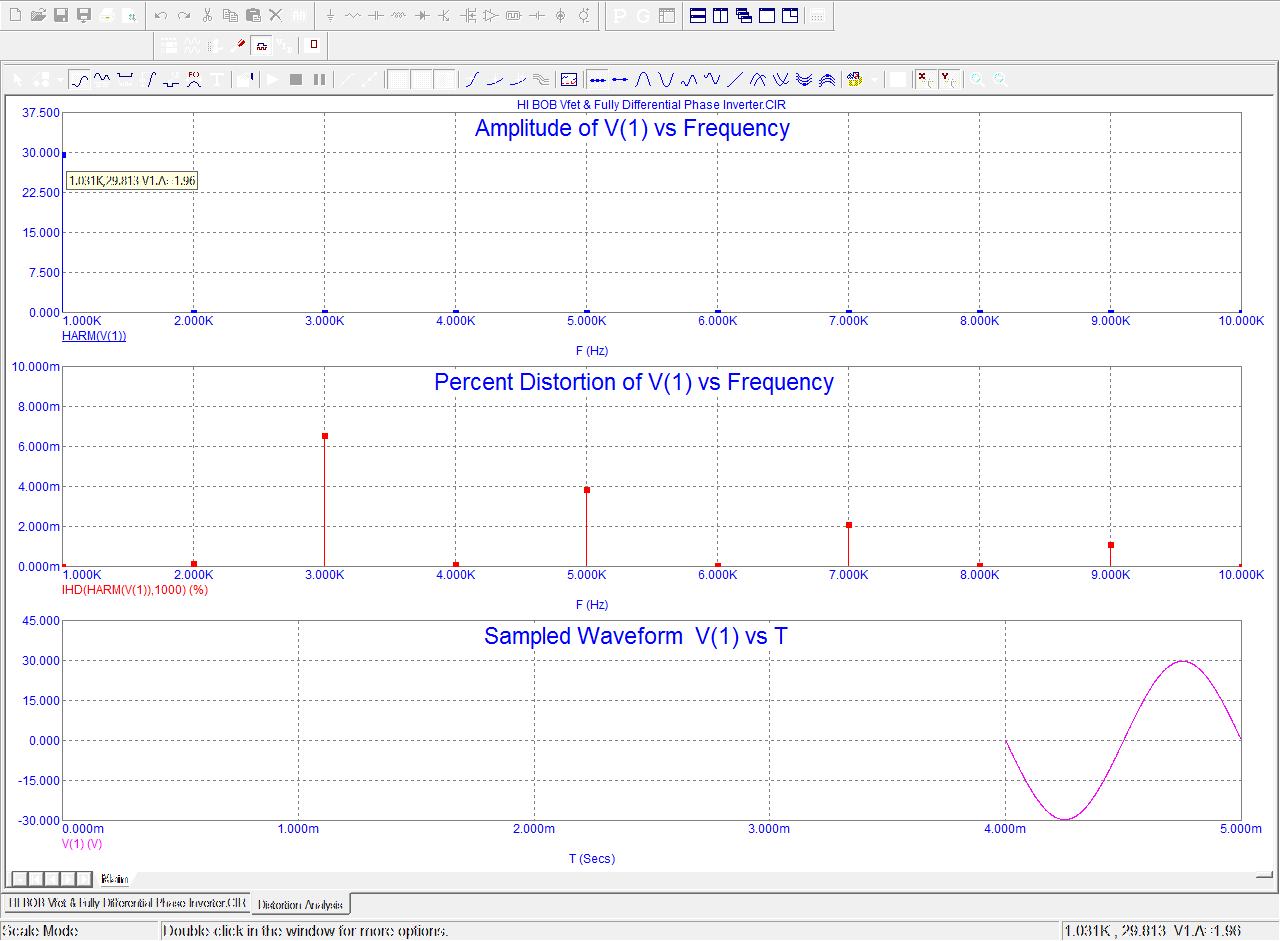
above: harmonic distortion at 28W
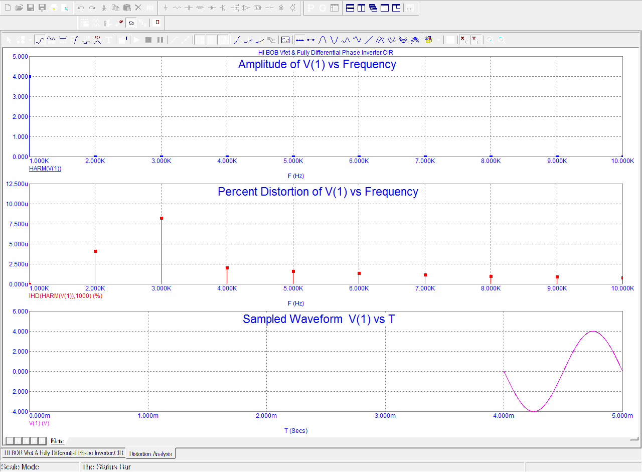
above: harmonic distortion at 50W
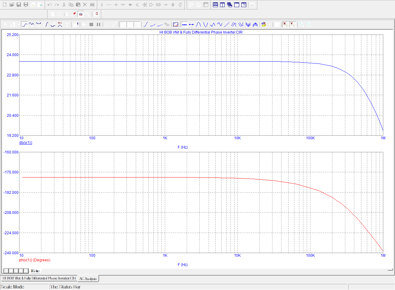
frequency and phase response
The third circuit is a direct derivation of the
second so called "HI BOB". The addition of HI specifies that it is a version
with a higher gain (open loop) than the version of the second circuit. Despite the higher level of GNFB adopted, it still remains very far from the high doses achieved by other circuits. The extreme linearity is MAINLY obtained with the choice of the devices and the best operating point work. It is in fact almost identical to the second schematic except for the addition of the two by-pass capacitors. The output power in this case reaches 55 W rms into 8 Ohms, with a very low distortion rate which extends up to 40 W rms / 8. Notes: This amp is designed for 8-ohm speakers. For loads less than that it is advisable to double output pairs. Consequently the achievable power could increase or doubling
above: harmonic distortion at 1W
above: harmonic distortion at 28W
above: harmonic distortion at 55W
trend of the frequency response and phase response
The fourth and last circuit,
although it is always dedicated to the achievement of a high linearity, it is
quite different in the logic.
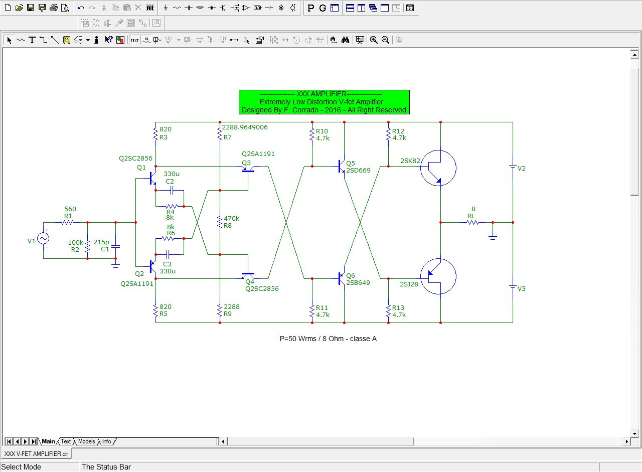
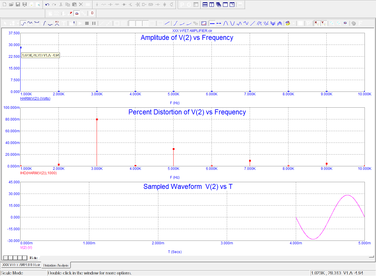
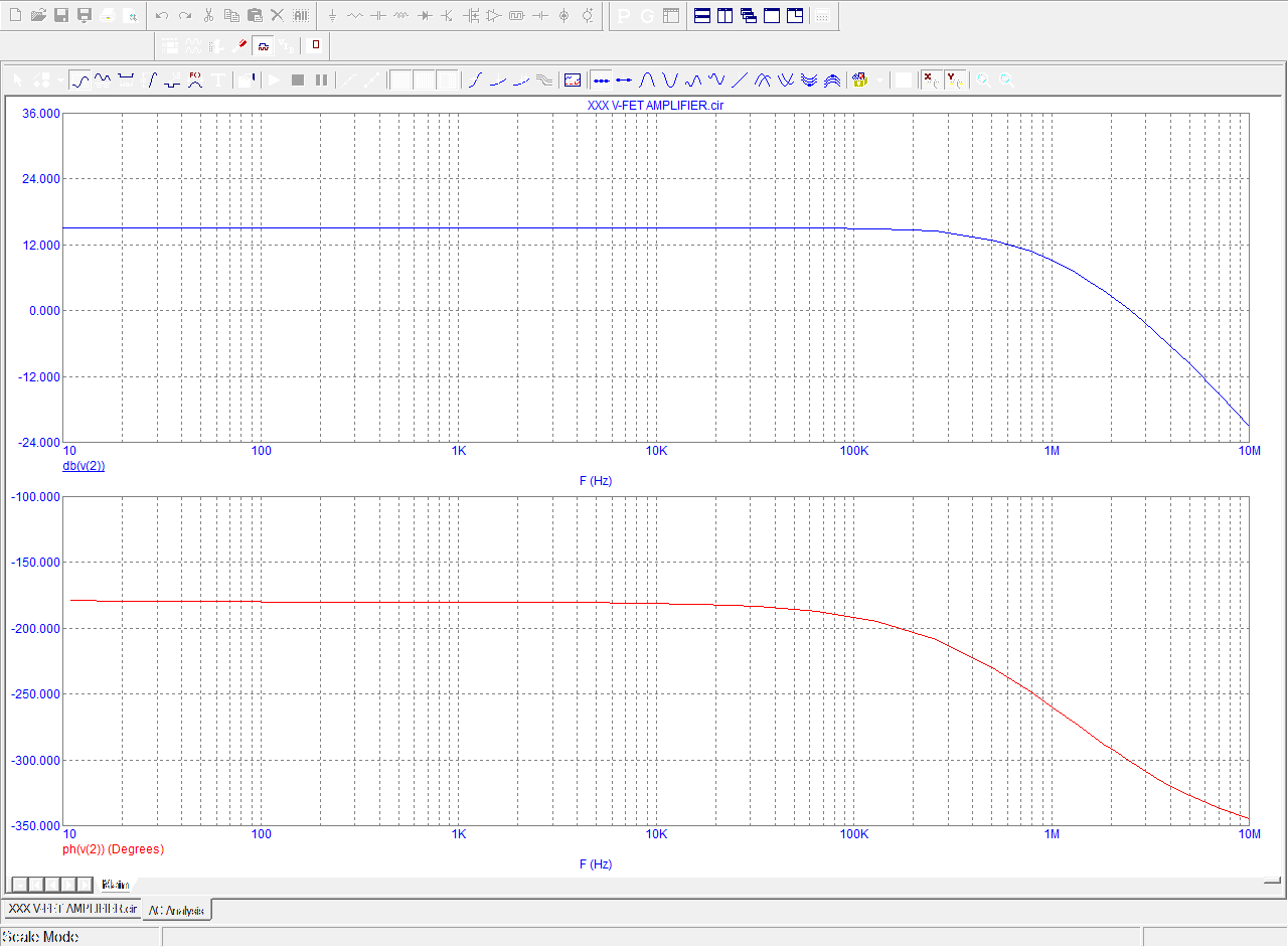
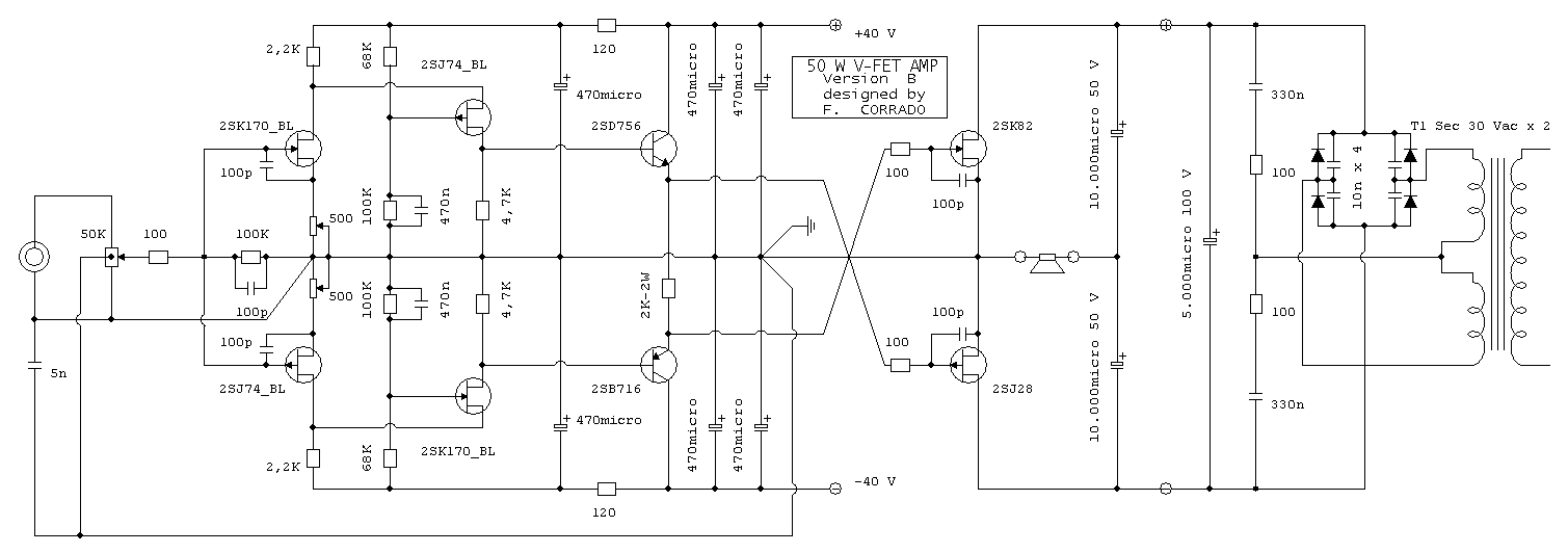
The schematic is a full complementary from input to output with a new design that is easy to recognize three X letters , hence the name given to this "XXX Amplifier". The sensitivity of this amplifier is quite low, so it is not recommended for everyone and is especially dedicated to the purists, those who appreciate circuits without the global feed-back, where performance measured mainly by instruments correspond to the actual performance, in a real system with real speakers and not artificial loads.
Notes: This scheme is optimized for use with 8 Ohm loads. In the case of use of 4-Ohm speakers, it is imperative to the doubling of the output devices. In this case, the output power could reach 100W.
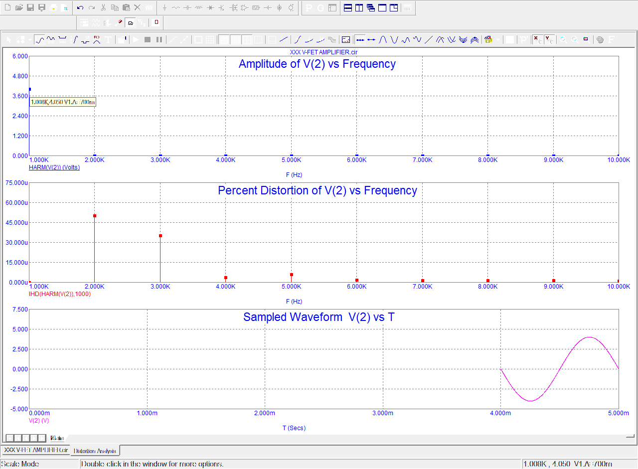
in the above: harmonic distortion at 1W
in the above: harmonic distortion at 10W
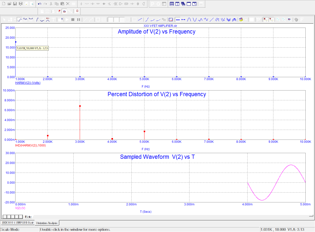
in the above: harmonic distortion at 20W
in the above: harmonic distortion at 50W
trend of frequency and phase response
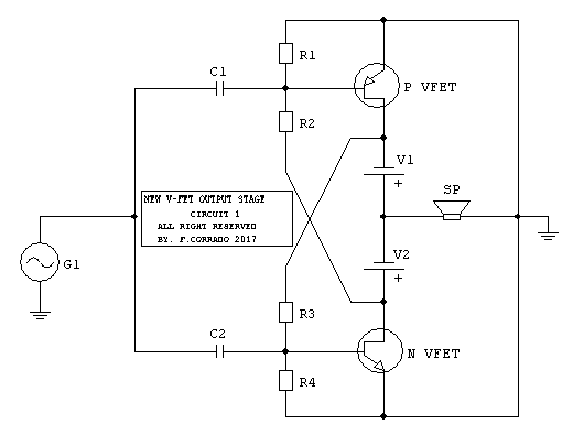
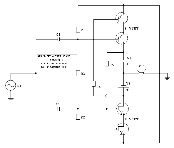
NEW V-FET OUTPUT STAGE
I In this scheme the Vfet output stage is capable of voltage
amplification despite the fact that only two power supplies are needed and not
four as I mentioned before, but despite this undoubted advantage some
technicians turn up their nose at the fact that the speaker is connected on one
side by means of two 10.000 microfarad electrolytic capacitors. This is a false
problem because in all amplifiers, even in the so-called direct coupled ones,
the audio current of the power stage always closes on the power supply
capacitors!!!!
here are the schematics I presented and wanted to name:
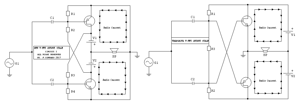
for complementary analogy to the already known Transnova stage
For a direct comparison between the new stage designed by me and the known trans-nova, I attach the following two diagrams with indicated the directions of audio currents circulation..
|
.jpg)